



1. Industry Background and Processing Challenges
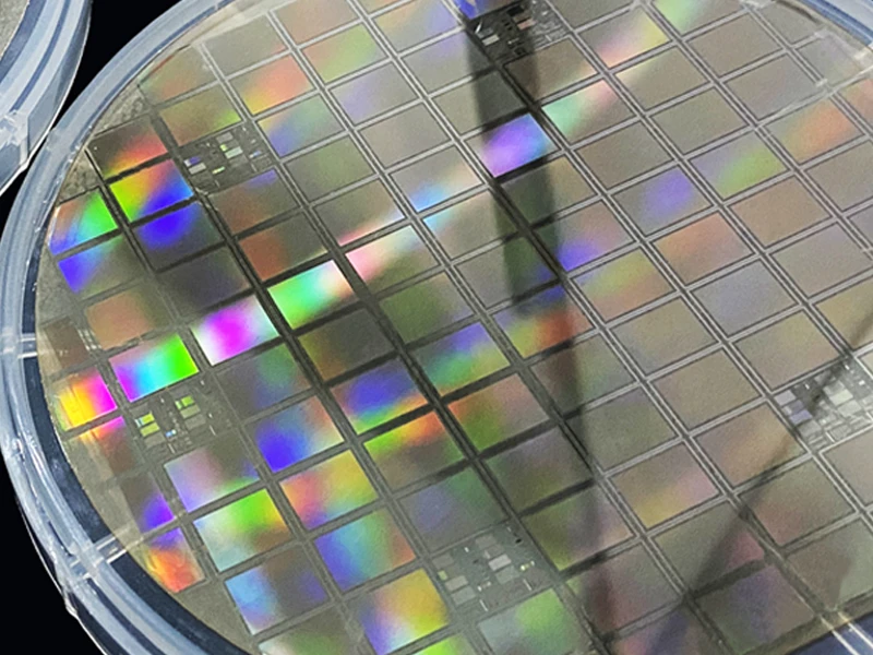
With the rapid advancement of three-dimensional (3D) packaging technology, the demand for ultra-thin chip fabrication has become increasingly urgent. In advanced packaging processes, silicon wafers must be thinned to the sub-100μm level to meet the stringent thickness and interconnect density requirements of stacked package architectures.
However, conventional mechanical grinding methods exhibit significant limitations when processing extremely thin wafers. Mechanical stress damage is inevitably introduced into the wafer bulk, generating lattice defects and micro-cracks. Simultaneously, warpage deformation intensifies dramatically as wafer thickness decreases, severely compromising alignment accuracy and yield in subsequent processes. These issues represent core bottlenecks in the ultra-thin chip manufacturing chain.
Laser thinning, as a non-contact processing approach, fundamentally avoids the introduction of mechanical contact stresses and is regarded as an important complement or even alternative to conventional grinding. Nevertheless, the complex thermal interactions between laser radiation and silicon material mean that the influence of process parameters on surface integrity remains insufficiently understood, necessitating systematic investigation.
2. Technical Approach: DOE-Assisted Rotary Laser Thinning
The core innovation of this process lies in the introduction of a Diffractive Optical Element (DOE) to perform wavefront shaping and energy distribution modulation of the laser beam. This homogenizes the energy distribution across the laser spot on the wafer surface, mitigating the localized over-ablation caused by the excessive peak intensity of a standard Gaussian beam profile.
Building upon this, the process employs a rotary scanning path, in which the laser beam traverses the wafer surface in spiral or concentric circular trajectories. Combined with programmable motion control, this enables precise regulation of the material removal process.
The study systematically investigated the effects of three core process parameters on wafer surface integrity:
Laser Power: Power governs the energy deposition per unit area and is the primary factor controlling material removal depth and the width of the heat-affected zone. Insufficient power yields inadequate removal efficiency, while excessive power leads to pronounced thermal accumulation, potentially inducing deep-seated cracks and recast layer formation.
Scanning Speed: Scanning speed controls the dwell time of the laser beam on the wafer surface, thereby determining local heat input. Higher scanning speeds reduce thermal accumulation but simultaneously decrease single-pass removal depth; lower speeds produce the opposite effect and must be co-optimized with power.
Overlap Rate: The degree of overlap between adjacent scan passes directly influences surface uniformity. An insufficient overlap rate leaves residual ridge-like protrusions between scan tracks, deteriorating surface roughness; an excessively high overlap rate amplifies thermal accumulation effects and may extend the depth of the heat-affected zone.
3. Mechanism of Laser–Silicon Material Interaction
Silicon is an indirect bandgap semiconductor material whose laser absorption characteristics are strongly wavelength-dependent. During laser irradiation, energy is converted from photon absorption into lattice thermal vibration, causing the temperature of the wafer surface and near-surface region to rise rapidly.
The material removal mechanism encompasses two primary stages: melting and vaporization. When the local temperature exceeds the melting point of silicon (approximately 1414°C), the material enters a molten state. With continued energy input, a portion of the melt further vaporizes and is expelled, resulting in macroscopic material removal. Residual melt solidifies rapidly once the laser beam moves away, forming a recast layer structure, which constitutes one of the key defect sources affecting surface integrity.
Concurrently, the Heat-Affected Zone (HAZ) generated by laser irradiation extends into the wafer depth. Within this region, the crystal structure undergoes varying degrees of phase transformation, dislocation proliferation, and amorphization, all of which adversely impact the mechanical strength and electrical properties of the wafer.
The evolution of surface morphology is closely coupled with process parameters. Under non-optimized conditions, the surface may exhibit periodic rippling, redeposition of ejected particulates, and micro-cracks. Within an optimized parameter window, however, these defects are effectively suppressed and the surface morphology approaches uniformity and flatness.
4. Process Optimization Objectives and Integration with CMP
Laser thinning does not target a final mirror-finish surface. Rather, it functions as a coarse thinning stage to provide a starting surface that meets the requirements of the subsequent Chemical Mechanical Planarization (CMP) process. Accordingly, the core constraints governing process optimization include:
Controlled material removal: Laser thinning must achieve precise approach toward the target thickness, ensuring a sufficient and uniform polishing allowance is preserved for CMP, while avoiding over-thinning that would expose damage layers beyond CMP’s corrective capacity.
Subsurface damage depth: The depth of the laser-induced heat-affected zone must be contained within the effective removal depth of the CMP process, ensuring that the damage layer is completely eliminated after CMP to yield a low-damage, polished final surface.
Surface roughness: The post-laser-thinning surface roughness must satisfy CMP feed requirements. Excessive surface topography variation significantly increases the difficulty and processing time required for CMP planarization.
Through the co-optimization of laser power, scanning speed, and overlap rate, the study established a qualified process parameter window satisfying the above constraints, achieving high-quality and controllable removal of thinned silicon wafers and laying the process foundation for integrated laser thinning and CMP workflows.
5. Technical Value and Application Prospects
The technical significance of this research manifests on two levels. At the process level, the study systematically elucidates the multi-parameter influence rules governing surface integrity in DOE-assisted rotary laser thinning, filling a critical gap in the laser thinning process database and providing parameter guidance for engineering applications. At the industrial level, the integrated laser thinning and CMP process route offers a viable pathway for ultra-thin chip fabrication that balances efficiency and surface quality, delivering direct engineering value to the advancement of advanced 3D packaging technology.