Who are we?
Wafering
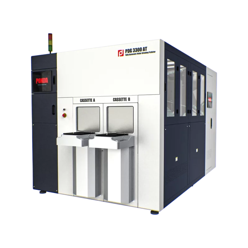
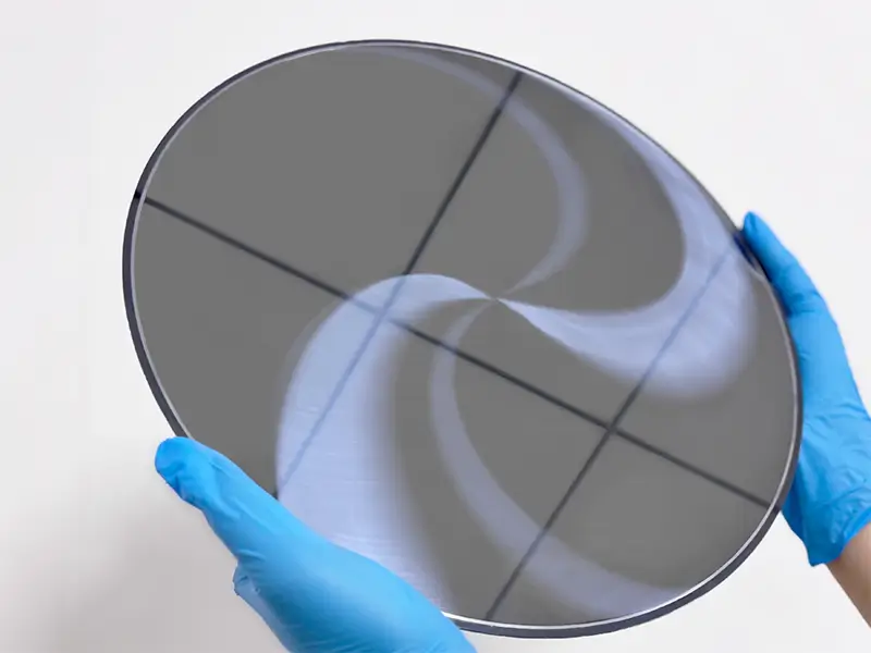
Wafering series focuses on producing thinner, higher precision semiconductor wafers.
Optics Surfacing
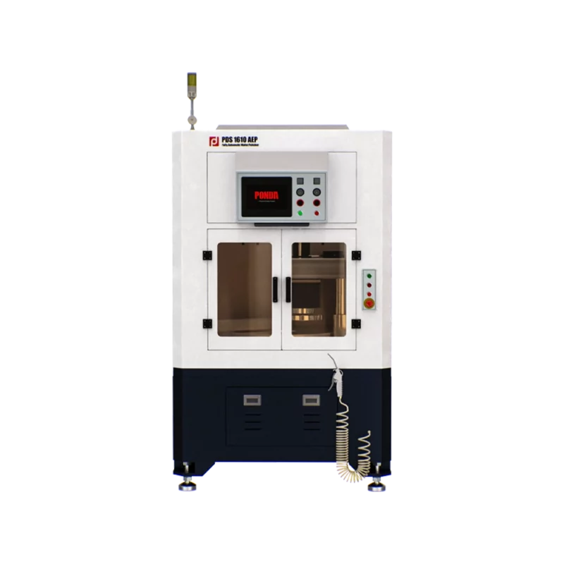
Optics surfacing series is applied to process spherical and aspherical workpieces such as lens.
Flat Finishing
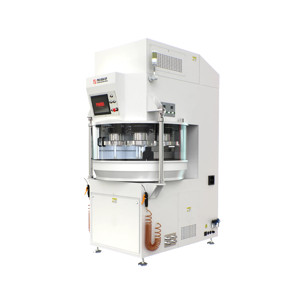
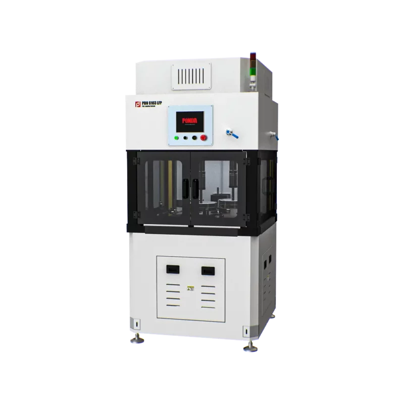
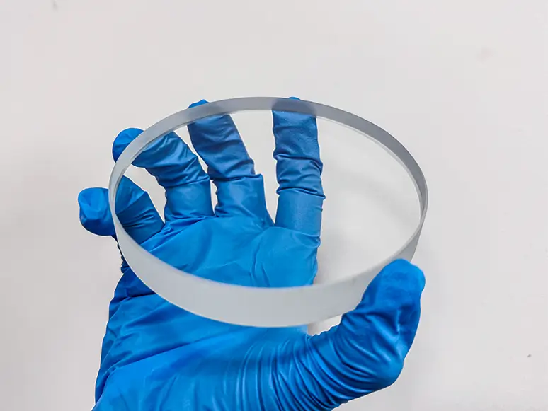
Flat lapping and polishing series are used to planarize various types of component and products.
Tools and Consuables
We develop and manufacture our own tools, ensuring complete control over equipment processing quality.
Why are Ponda's machines used for processing?
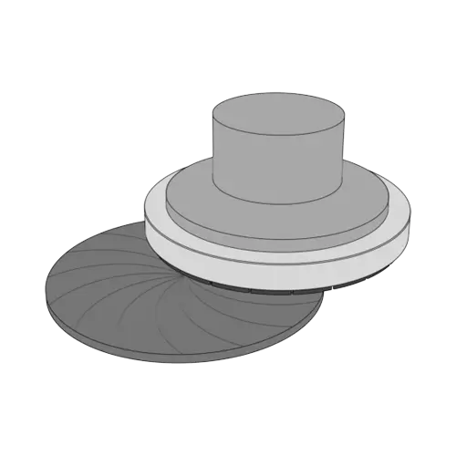
Wafers with TAIKO Ring
Wafering
In semiconductor manufacturing, users require thinner, more uniform wafers with higher yield to be packaged into chips. Therefore, the Wafering series is specifically developed to meet these needs.
Optical Lens
Spherical and Aspherical Processing
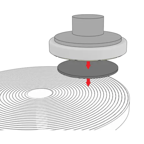
In optical machining, multi-axis CNC equipment is usually required to process spherical or aspherical lenses in order to achieve ultra-precise control over the shape of the workpiece.
Precision Mold
Flat Finishing
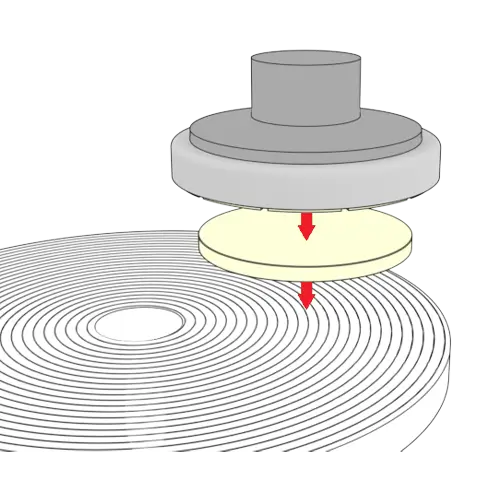
Products like static-pressure bearing and linear slider, high-precision optical lens, sealing valve, benchmark block require flat finishing equipment.
Where are Ponda's machines used in semiconductor industry?
Our semiconductor equipment is mainly used in wafer manufacturing and wafer fabrication for grinding and polishing, as well as in post-packaging grinding. We also produce supporting equipment to complete the processing chain.
Wafer Manufacturing

Ingot Slicing

Chamfering

Grinding
Wafer Fabrication

Patterned Wafer

Backgrinding

CMP Finishing
The edges of sliced wafers are sharp and fragile. By applying edge beveling to form arc-shaped profiles, stress concentration points are eliminated.
The surface of a sliced wafer is not flat. Through grinding, the wafer can be thinned while achieving improved flatness.
Backgrinding thins the wafer while protecting the circuits. Subsequently, CMP is used to remove the remaining damage layer and planarize the wafer. The thinned wafer also reduces stress damage during dicing.
Sapphire, GaN Manufacturing

Wax Mounting

Grinding
Lapping & Polishing

Patterned Wafer

CMP Finishing
Wafering Fabrication

Backgrinding

CMP Finishing
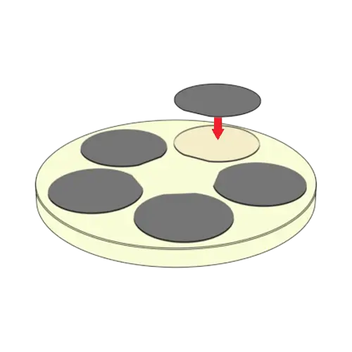
Sapphire wafers have high brittleness, and wax bonding is used to prevent surface cracks or edge chipping. This also significantly reduces deformation during processing and ensures good yield and precision in subsequent processes.
After sapphire grinding, lapping is used to reduce the damage layer left by grinding and further improve surface roughness, enhancing the efficiency of polishing. Polishing then completely removes the damage layer and achieves a smooth and shinny surface.
During the backgrinding stage of sapphire wafers, specially-made films are used to protect the circuits. The thinning process ends after lapping and CMP finishing.