



1. Background and Challenges
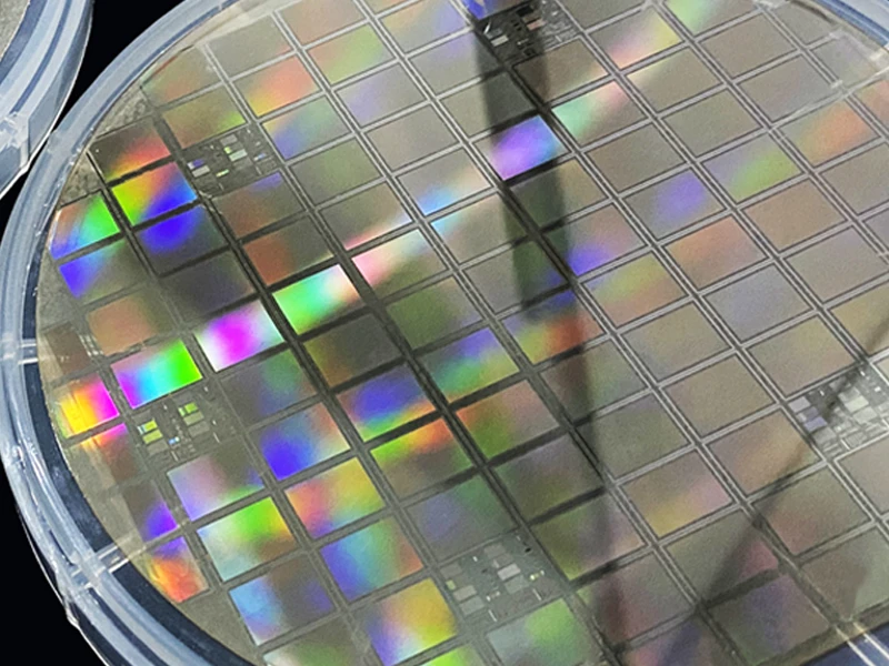
Single-crystal silicon is an indispensable core material in modern integrated circuit manufacturing. Its surface and subsurface quality directly determines the electrical performance and service life of the final devices. During silicon wafer thinning and grinding processes, Subsurface Damage (SSD) represents a critical bottleneck that constrains wafer yield in subsequent processing steps. Conventional grinding inevitably introduces crystal defects and micro-cracks into the subsurface layer, seriously affecting the reliability of subsequent CMP polishing and device fabrication.Although nano-grinding technology can control surface roughness to the nanometer scale, the intrinsic relationship between SSD formation mechanisms, mechanical response, and thermal behavior at the atomic scale has long lacked a clear understanding, which has hindered further process optimization.
2. Core Mechanisms: Structural Phase Transformation and Amorphization
The research employed Molecular Dynamics (MD) simulation to construct a precise model of single-crystal silicon nano-grinding at the atomic scale, systematically revealing the dominant formation mechanisms of SSD.
The study clearly identified two core mechanisms responsible for SSD formation during nano-grinding: structural phase transformation and amorphization. Under the highly localized contact between abrasive grains and the silicon lattice, silicon atoms are subjected to extreme shear stress, causing the crystal structure to undergo phase transformation from the diamond cubic structure to a metastable phase, ultimately forming an amorphized region in the subsurface layer as the fundamental source of damage.
Furthermore, the study established that tangential grinding force plays a dominant role in the material removal process, with its magnitude and direction directly determining the material removal mode and both the depth and extent of subsurface damage.
3. Influence of Force-Thermal Behavior on Subsurface Damage
Grinding depth and grinding speed are the two most critical process parameters influencing force-thermal behavior, and each exerts distinct effects on SSD formation.
As grinding depth increases, the contact area between the abrasive and workpiece expands, causing both tangential and normal forces to rise simultaneously. The heat generated in the grinding zone increases significantly, leading to a corresponding aggravation of subsurface damage depth.
As grinding speed increases, grinding heat also rises. However, the research revealed a key counter-intuitive phenomenon: a moderate temperature elevation can enhance the material toughness of single-crystal silicon, promoting plastic flow rather than brittle fracture during material removal, thereby improving subsurface quality to a certain degree. This finding provides important theoretical guidance for process optimization.
4. Atomic Mobility and Surface Stress Concentration Mechanism
The research further revealed the SSD initiation pathway from the perspective of atomic motion. Under the influence of grinding heat, the atomic mobility of silicon undergoes significant changes, and the non-uniformity in local atomic arrangement leads to stress concentration on the wafer surface layer. Once this stress concentration exceeds the local fracture toughness threshold of the material, micro-crack initiation and propagation are triggered, ultimately forming detectable subsurface damage.
The clarification of this mechanism closely links macroscopic force-thermal parameters with microscopic atomic behavior, providing a theoretical closed loop for actively intervening in SSD formation through process control.
5. Process Control Strategies and Practical Recommendations
Based on the above mechanistic findings, the following process control pathways for effectively suppressing SSD in single-crystal silicon nano-grinding are proposed:
Reducing grinding depth is the most direct means of minimizing SSD. A smaller depth of cut implies lower contact stress and a shallower damage layer, which is conducive to preserving wafer subsurface integrity.
Appropriately increasing grinding speed can enhance material toughness through the temperature rise effect, promoting plastic-mode material removal and thereby suppressing the generation of brittle cracks to improve subsurface quality.
The synergistic optimization of both parameters — specifically, combining small grinding depth with higher grinding speed — is the recommended strategy for achieving minimum subsurface damage while maintaining acceptable processing efficiency.
6. Conclusion
This study systematically revealed the SSD formation mechanism in single-crystal silicon nano-grinding at the atomic scale, identifying structural phase transformation and amorphization as the dominant damage mechanisms. It clarified the role of force-thermal coupling behavior on subsurface quality and proposed a process strategy for synergistically controlling SSD through reduced grinding depth and elevated grinding speed. These findings provide a solid theoretical foundation for the design of high-quality grinding and thinning processes for semiconductor silicon wafers, offering significant engineering guidance for improving wafer processing yield in integrated circuit manufacturing.