
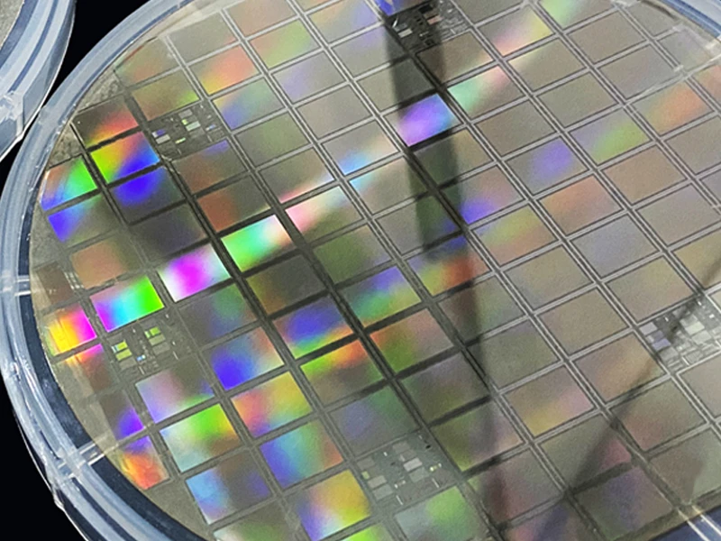


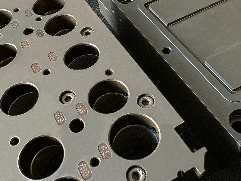

As chips become thinner, wafer backside grinding for thicknesses below 200 μm often leads to catastrophic breakage. Wafers may crack along grinding marks, split along crystal planes, or shatter completely. Not only are entire batches scrapped, but extensive troubleshooting also cripples productivity and increases costs. Even after adjusting grinding wheels, RPM, and feed rates, breakage recurs unpredictably.
This article breaks down the three most common failure modes in wafer backside grinding—including definitions, root causes, and field-proven corrective solutions from OEMs.
Ⅰ. Cracking Along Grinding Marks
Typical wheel-related issue, frequent for wafers below 200 μm
What is cracking along grinding marks?
“Grinding marks” are the abrasive traces left by the grinding wheel on the wafer surface during backgrinding. Cracking along these marks is one of the most prevalent failure modes.
The root cause is poor grinding performance—such as clogged chip pockets or insufficient abrasive capability—creating excessive stress that causes the wafer to split along grinding paths. For ultra-thin wafers <200 μm, this issue escalates when combined with uncut tape or pre-existing edge cracks.
4 Core Causes & OEM Solutions
- Insufficient grinding capability of Z1 rough grinding wheelEspecially severe for wafers with thick oxide films, due to mismatched wheel specifications.✅ Solution: Use a more aggressive wheel with larger abrasive grain size and higher-performance bond.
- Water leakage at wheel‑hub interfaceReduces coolant flow, impairs cooling and chip removal, and degrades grinding stability.✅ Solution: Clean the wheel‑hub mounting surface, ensure gap‑free contact, and eliminate leakage.
- Clogged wheel chip pocketsDebris from uncut tape or swarf lodges in wheel gaps during finish grinding, drastically increasing wafer stress.✅ Solution: Perform timely wheel dressing to clear clogged pockets and restore grinding performance.
- Grinding-induced edge crack propagationEdge microcracks catch between wheel and wafer, causing cracks to extend along grinding marks.✅ Solution: Reduce cooling water flow rate to minimize hydrodynamic impact on wafer edges.
Critical reminder:
For wafers thinned to 200 μm and below, causes 3 and 4 become dominant failure points and require extra inspection.
Ⅱ. Cleavage Along Crystal Planes
Unrelated to grinding wheels! 90% caused by foreign contamination
What is cleavage along crystal planes?
Silicon wafers have fixed crystallographic orientations. Cleavage along these planes produces straight, directional cracks. Non-crystallographic linear cracking may occur in rare cases.
3 Core Causes & OEM Solutions
This failure stems entirely from foreign particles creating uneven pressure during grinding.
- Particles on chuck surface✅ Solution: Thoroughly clean the chuck top surface to remove all particles and swarf.
- Particles trapped between chuck and wafer (tape)✅ Solution: Inspect chuck and tape before mounting; press gently to ensure uniform contact.
- Particles on transfer padsContaminants transfer to wafer/tape during handling and enter the grinder.✅ Solution: Regularly clean wafer transfer pads to maintain particle-free surfaces.
Supplementary note:
“Foreign particles” include both external contaminants and silicon swarf generated during grinding. Daily cleaning is essential.
Ⅲ. Irregular Shattering
Random breakage linked to equipment handling and wafer transport
What is irregular shattering?
Breakage follows no grinding marks or crystal directions, ranging from random cracks to complete fragmentation. This is the most damaging failure mode in backside grinding, especially for thin wafers.
2 Core Causes & OEM Solutions
- Collision with peripheral components during handlingMisaligned or improperly spaced parts cause hidden cracks during loading/unloading, which propagate during grinding.✅ Solution: Inspect and adjust grinder peripherals to ensure safe clearance for wafer transport.
- Insufficient wafer strength (finish grinding stage)Below 200 μm, wafer strength drops sharply. Combined with prior failure triggers (contamination, poor grinding), it shatters randomly.✅ Solution: Eliminate causes from Types Ⅰ and Ⅱ—especially chuck contamination—before finish grinding.
Critical reminder:
Irregular breakage in <200 μm wafers is not always from crystallographic causes. Analyze fracture patterns and handling paths before making blind adjustments.
OEM Ultimate Troubleshooting Guide
Follow this sequence to identify root causes and avoid 90% of wasted effort:
- Crack pattern first:Along grinding marks → check wheel/grinding parametersAlong crystal planes → check foreign contaminationRandom → check peripherals/handling
- For <200 μm thin grinding:Focus on clogged chip pockets, edge cracks (Type Ⅰ), and strength-related shattering (Type Ⅲ)
- Elimination order:Simple fixes first (cleaning, dressing, coolant) → complex changes (wheel replacement, part alignment)
- Special conditions:For thick oxide films or exotic materials, contact your OEM representative for customized solutions.
Conclusion
Breakage in thin wafer backgrinding rarely stems from a single factor—it usually results from overlooked details: neglected chuck cleaning, delayed wheel dressing, or excessive coolant flow.
Grinding yield depends not on premium wheels or perfect parameters, but on standardized, detail‑oriented basic operations: regular equipment cleaning, timely wheel dressing, and careful wafer mounting.
For engineers working on wafer backside grinding and chip thinning, save and share this guide. Next time wafers break, use this systematic approach instead of blind tuning—protect wafers, stabilize processes, and boost grinding yield!