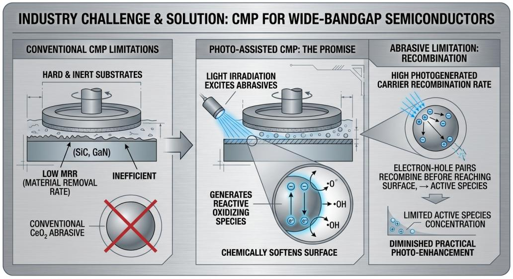
1. Background and Industry Challenges
Chemical mechanical polishing (CMP) serves as the critical process for achieving global planarization of wafer surfaces in semiconductor manufacturing. When it comes to wide-bandgap semiconductor materials such as SiC and GaN, conventional CMP processes face severe limitations due to the extreme hardness and chemical inertness of these substrates, resulting in prohibitively low material removal rates (MRR) that significantly constrain manufacturing efficiency and economics.To overcome this bottleneck, photo-assisted CMP has emerged as a promising technology. Its fundamental principle lies in utilizing light irradiation to excite photogenerated electron-hole pairs within the abrasive particles, generating highly reactive oxidizing species at the polishing interface. These species chemically soften the workpiece surface, substantially reducing the mechanical removal barrier. However, conventional single-phase CeO₂ abrasives suffer from a fundamental limitation: an extremely high photogenerated carrier recombination rate. The majority of electron-hole pairs recombine before reaching the abrasive surface, resulting in a concentration of active species far below the theoretical optimum and severely diminishing the practical photo-enhancement effect.
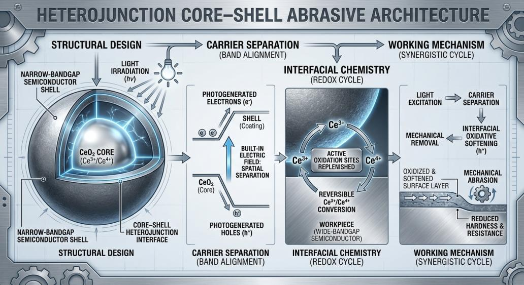
2. Core Technical Approach: Heterojunction Core–Shell Abrasive Architecture
To address this challenge, researchers developed a heterojunction-enhanced CeO₂ core–shell abrasive design strategy that fundamentally resolves the carrier recombination issue.
From a structural design perspective, CeO₂ particles serve as the inner core, coated with a narrow-bandgap semiconductor material possessing a complementary band structure, thereby forming a well-defined core–shell heterojunction interface. The proper alignment of band positions between the two materials is the critical prerequisite for effective heterojunction operation. Under light irradiation, a built-in electric field is established at the heterojunction interface, driving photogenerated electrons and holes to migrate in opposite directions. This achieves spatial separation of charge carriers, effectively suppressing recombination.
From an interfacial chemistry perspective, the inherent Ce³⁺/Ce⁴⁺ redox cycling mechanism of CeO₂ is further synergistically enhanced at the core–shell interface. The reversible conversion between Ce³⁺ and Ce⁴⁺ continuously replenishes active oxidation sites at the polishing interface, maintaining consistently high chemical reactivity at the abrasive surface. This represents a unique advantage of CeO₂-based systems that distinguishes them from other abrasive platforms.
From a working mechanism perspective, under illumination, the heterojunction structure continuously injects photogenerated holes into the contact interface between the abrasive and the workpiece. These holes, possessing strong oxidizing capability, oxidize and chemically soften the surface layer of the wide-bandgap semiconductor workpiece, substantially reducing its hardness and resistance to removal. This renders subsequent mechanical abrasion far more efficient. The entire process forms a highly synergistic cycle of: light excitation → carrier separation → interfacial oxidative softening → mechanical removal.
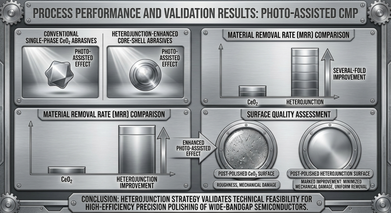
3. Process Performance and Validation Results
Comparative photo-assisted CMP experiments conducted on wide-bandgap semiconductor materials demonstrated that the heterojunction-enhanced core–shell abrasives significantly outperformed conventional single-phase CeO₂ abrasives across key performance metrics.
In terms of material removal rate (MRR), the heterojunction abrasives achieved a several-fold improvement over single-phase CeO₂, directly validating the substantially enhanced photo-assisted effect.
In terms of surface quality, the post-polished workpiece surfaces showed marked improvement, indicating that more efficient chemical softening facilitates gentler and more uniform material removal while minimizing mechanical damage to the surface.
These experimental results collectively validate the technical feasibility of the heterojunction strategy in photo-assisted CMP, providing a practically viable technical pathway for the high-efficiency precision polishing of wide-bandgap semiconductor materials.
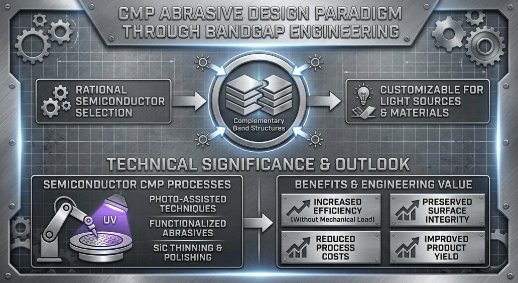
4. Technical Significance and Outlook
The significance of this research extends beyond the introduction of a high-performance abrasive. More importantly, it establishes a design paradigm for enhancing the photocatalytic efficacy of CMP abrasives through bandgap engineering. By rationally selecting semiconductor combinations with complementary band structures, the approach can be customized for different light sources and workpiece materials, offering considerable technical versatility and extensibility.For Panda’s practical applications in semiconductor CMP processes, this research points to an important strategic direction. When processing wide-bandgap substrates such as SiC during thinning and polishing operations, incorporating photo-assisted techniques in conjunction with functionalized abrasives holds the potential to substantially increase processing efficiency without increasing mechanical load, while simultaneously preserving surface integrity. This carries direct engineering reference value for reducing process costs and improving product yield.