
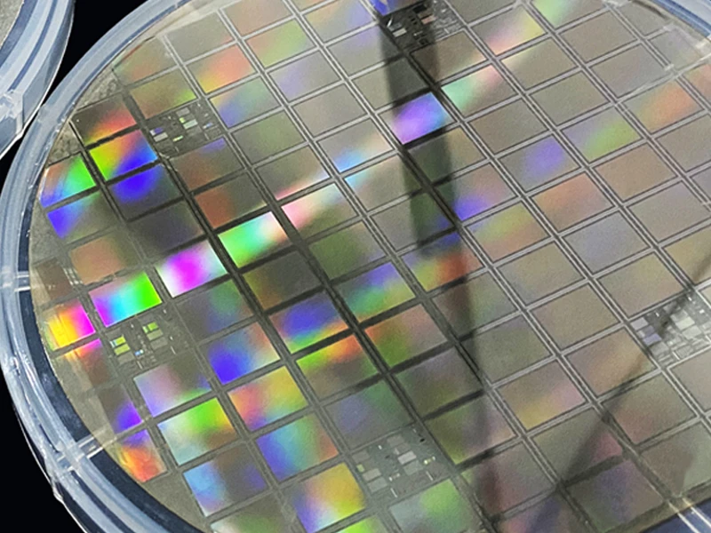



Backside Metallization (back metal process) is a semiconductor manufacturing process that deposits a metal layer on the backside of a wafer or die. As a key step in semiconductor packaging and fabrication, its primary purpose is to improve heat dissipation, mechanical stability, and electrical interconnection via the metal layer, ensuring high reliability and efficiency of the chip.
Core Functions of Backside Metallization
In semiconductor devices — especially power devices and high-performance chips — backside metallization is critical, with three main functions:
1. Improve Thermal Dissipation Performance
Chips generate considerable heat during operation. Depositing a high-thermal-conductivity metal layer (such as Au or Ag) on the backside greatly boosts heat conduction, quickly transferring heat to the package or heat sink.
2. Enhance Mechanical Stability
Thinned wafers have low mechanical strength and are prone to stress-induced cracking. The backside metal layer reinforces structural strength and reduces the risk of breakage.
3. Enable Electrical Connection and Bonding
The backside metal layer serves as a stable electrical contact and bonding base. It forms reliable electrical and mechanical connections with package substrates or lead frames via solder paste or conductive adhesive, providing a low-resistance path for current and signal output.
Main Process Flow of Backside Metallization
Step 1: Protective Film Lamination
A protective film is applied to the frontside of the wafer to prevent damage to the circuit patterns during subsequent grinding, etching, and cleaning.
Step 2: Wafer Backside Thinning
The wafer backside is thinned to the target thickness using mechanical grinding. Thinning reduces thermal resistance, improves heat dissipation, and meets packaging thickness requirements while maintaining thickness uniformity.
Step 3: Silicon Etching
After grinding, the wafer surface contains a damaged layer and residual stress. Chemical etching (typically HF + HNO₃) removes the damaged layer, releases stress, and increases surface roughness to improve metal adhesion.
Step 4: Cleaning and Pretreatment
The backside is thoroughly cleaned to remove native oxide, particles, and chemical residues, which is critical for strong adhesion between metal and silicon.
Step 5: Backside Metallization Deposition
This is the core step, usually performed by physical vapor deposition (PVD) such as electron-beam evaporation. Multiple metal thin films are sequentially deposited in a vacuum chamber.
Typical Back Metal Layer Structure and Material Selection
To achieve strong adhesion, diffusion barrier, and good solderability, the back metal layer generally uses a multi-layer structure:
Layer 1: Adhesion Layer
Directly contacts the silicon substrate, providing excellent bonding strength and ohmic contact.
Common materials: Ti, Cr.
Layer 2: Barrier Layer
Prevents inter-diffusion between upper and lower metals and avoids high-resistance compounds.
Common materials: Ni, NiV alloy.
Layer 3: Anti-oxidation / Solder Layer
The outermost layer with high conductivity, thermal conductivity, oxidation resistance, and good wettability with solder.
Common materials: Au, Ag.
In high-end applications, more complex structures including seed layers are used for high-temperature and high-power conditions.
Technical Characteristics and Applications
Advantages
- Greatly improves chip heat dissipation and lowers operating temperature
- Enhances mechanical strength and packaging reliability
- Provides stable, low-resistance backside electrical contact
- Protects the wafer backside from contamination
- Supports vacuum mounting and advanced packaging
Challenges
- High process cost due to specialized equipment and high-end materials
- Strict control requirements for vacuum and cleanliness
- Risk of defects such as metal peeling and sputtering
- Minor influence on ultra-sensitive electrical parameters in some cases
Main Applications
- Power semiconductors: IGBT, MOSFET for EV controllers, inverters
- High-end computing chips: CPU, GPU
- LED packaging: improved thermal performance and lifespan
- Solar panels: enhanced efficiency and long-term reliability
As semiconductors trend toward higher power density, smaller size, and higher integration, backside metallization will continue to evolve in materials, process precision, and integration schemes.