


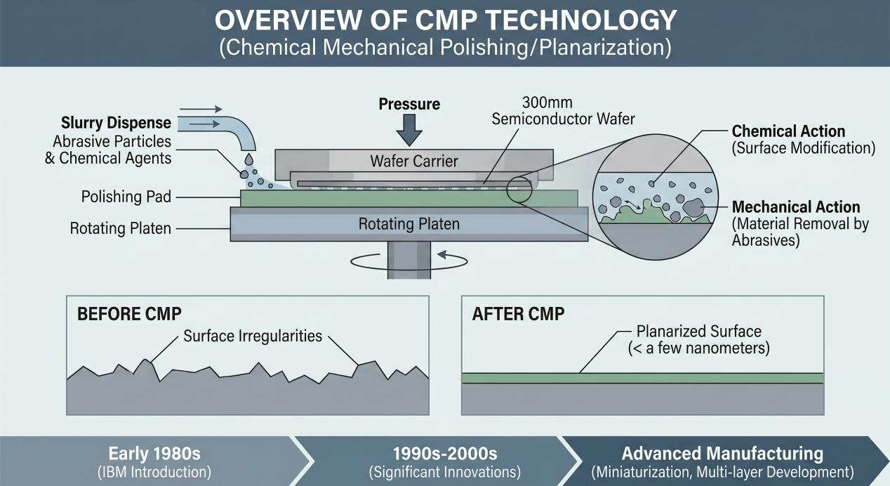
1. Overview of CMP Technology
CMP (Chemical Mechanical Polishing/Planarization) is a critical process technology in advanced semiconductor manufacturing that reduces surface irregularities on 300mm wafers to below several nanometers. The technology was born in the early 1980s, first introduced by IBM as an extension of polishing equipment used in bare wafer manufacturing.As the name implies, CMP achieves wafer polishing through the synergistic action of chemical and mechanical factors. Its planarization precision holds an absolute advantage over other methods. The technology underwent significant innovations during the 1990s to 2000s, enabling the miniaturization and multi-layer development of semiconductor devices.
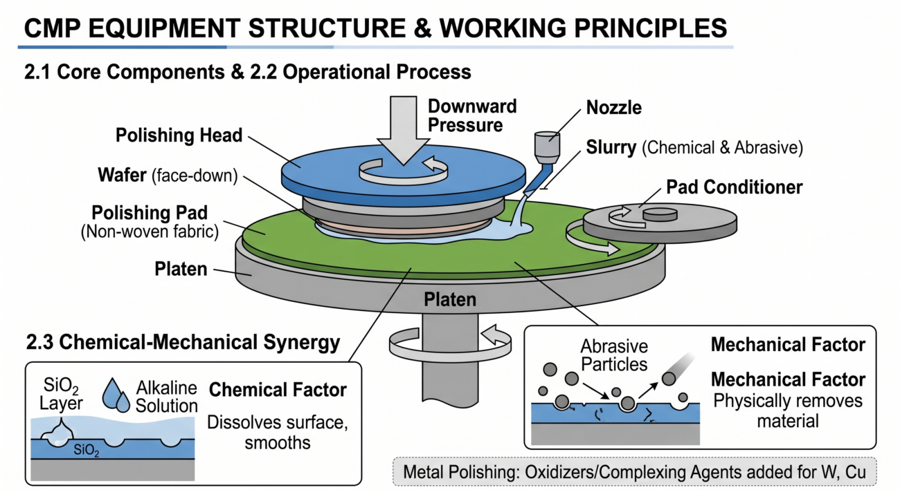
2. Basic Structure and Working Principles of CMP Equipment
2.1 Core Components
A CMP system consists of the following key components:
Polishing Head: Holds the wafer, applies downward pressure, and rotates
Platen: Mounts the polishing pad made of non-woven fabric, rotates synchronously
Polishing Pad: Non-woven fabric material providing the mechanical polishing interface
Nozzle: Dispenses chemical solutions or slurry
Pad Conditioner: Restores polishing pad performance by removing clogging
2.2 Operational Process
During operation, the wafer is loaded face-down into the polishing head. Moderate downward pressure is applied while the polishing head rotates for polishing, with the platen rotating simultaneously.
2.3 Chemical-Mechanical Synergy
Chemical factor: For example, when removing insulating SiO₂ layers, an alkaline solution capable of dissolving SiO₂ smooths the surface
Mechanical factor: Abrasive particles in the slurry physically remove materialMetal polishing: When polishing tungsten (W) or copper (Cu) interconnects, oxidizers or complexing agents are typically added to the slurry
3. Development History of CMP Technology
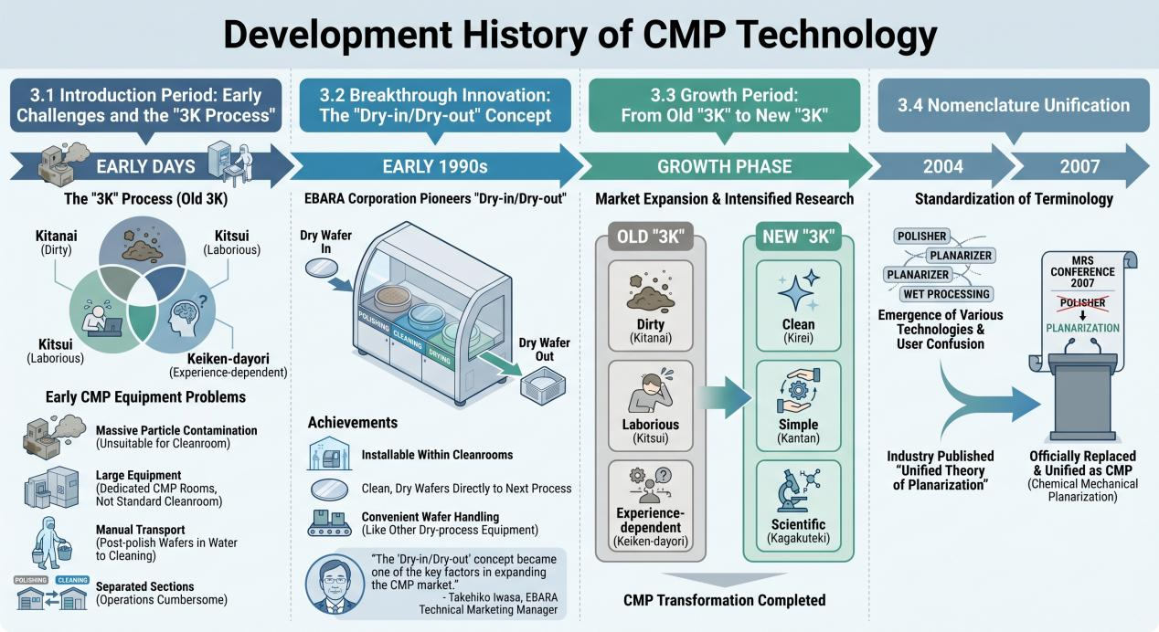
3.1 Introduction Period: Early Challenges and the “3K Process”
In its early days, CMP was regarded as the “3K process” — Kitanai (dirty), Kitsui (laborious), and Keiken-dayori (experience-dependent) — completely incompatible with the clean semiconductor manufacturing environment.
Early CMP equipment faced the following problems:
The polishing process generated massive particle contamination, making it unsuitable for cleanroom use
Large equipment could not fit in standard cleanrooms, requiring dedicated CMP rooms
Post-polish wafers had to be placed in water and manually transported to cleaning equipment
Polishing and cleaning sections were separated, making operations cumbersome
3.2 Breakthrough Innovation: The “Dry-in/Dry-out” Concept
EBARA Corporation pioneered the “Dry-in/Dry-out” concept, completing polishing, cleaning, and drying within the equipment while containing contamination internally. This innovation achieved:
CMP equipment installable within cleanrooms
Clean, dry wafers sent directly to the next process
Wafer handling as convenient as other dry-process equipment
EBARA’s Technical Marketing Manager, Takehiko Iwasa, stated: “The ‘Dry-in/Dry-out’ concept became one of the key factors in expanding the CMP market.”
3.3 Growth Period: From Old “3K” to New “3K”
With the proliferation of the “Dry-in/Dry-out” concept and market expansion, companies and universities intensified research efforts. CMP completed its transformation from the old “3K” to the new “3K”:
Old “3K”
New “3K”
Dirty (Kitanai)
Clean (Kirei)
Laborious (Kitsui)
Simple (Kantan)
Experience-dependent (Keiken-dayori)
Scientific (Kagakuteki)
Old “3K”
New “3K”
Dirty (Kitanai)
Clean (Kirei)
Laborious (Kitsui)
Simple (Kantan)
Experience-dependent (Keiken-dayori)
Scientific (Kagakuteki)
3.4 Nomenclature UnificationAround 2004, the emergence of various planarization technologies caused user confusion. The industry published the “Unified Theory of Planarization” to integrate all wet planarization equipment technologies. At the 2007 MRS conference, Polisher was officially replaced with Planarization, unifying the terminology as CMP (Planarization).
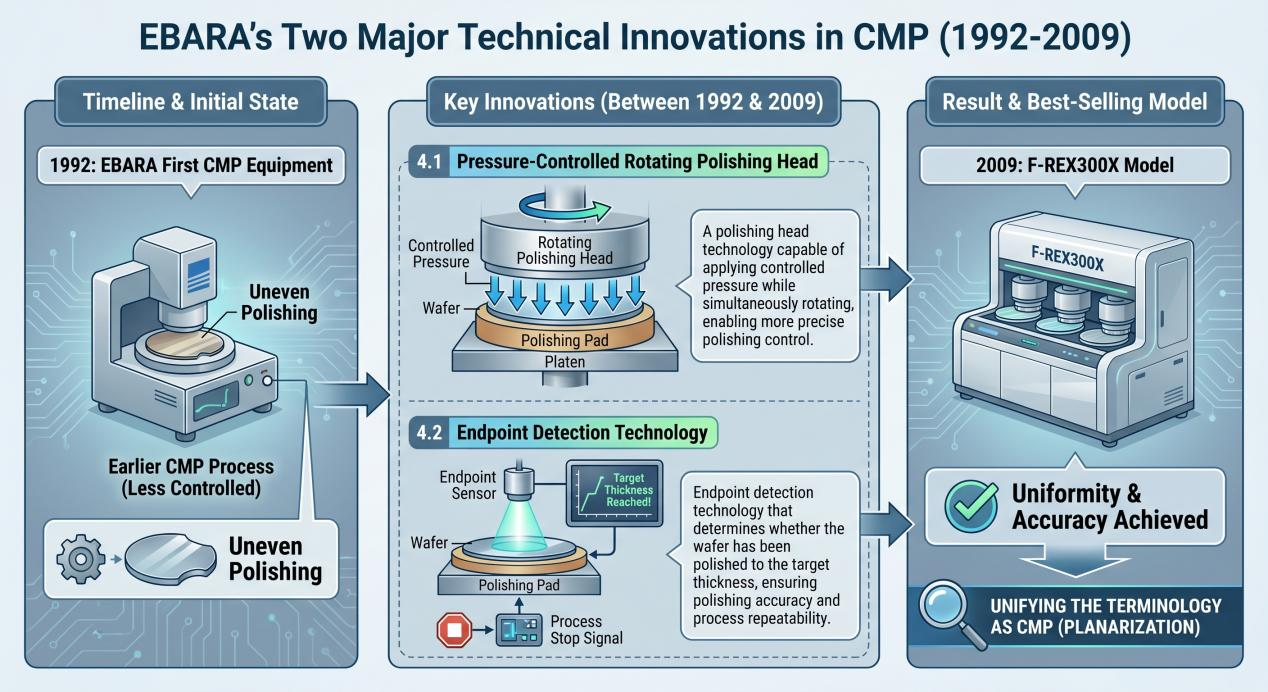
4. EBARA’s Two Major Technical Innovations
EBARA introduced its first CMP equipment in 1992. Between then and the 2009 release of its best-selling “F-REX300X” model, two key technical innovations occurred:
4.1 Pressure-Controlled Rotating Polishing Head
A polishing head technology capable of applying controlled pressure while simultaneously rotating, enabling more precise polishing control.
4.2 Endpoint Detection TechnologyEndpoint detection technology that determines whether the wafer has been polished to the target thickness, ensuring polishing accuracy and process repeatability.
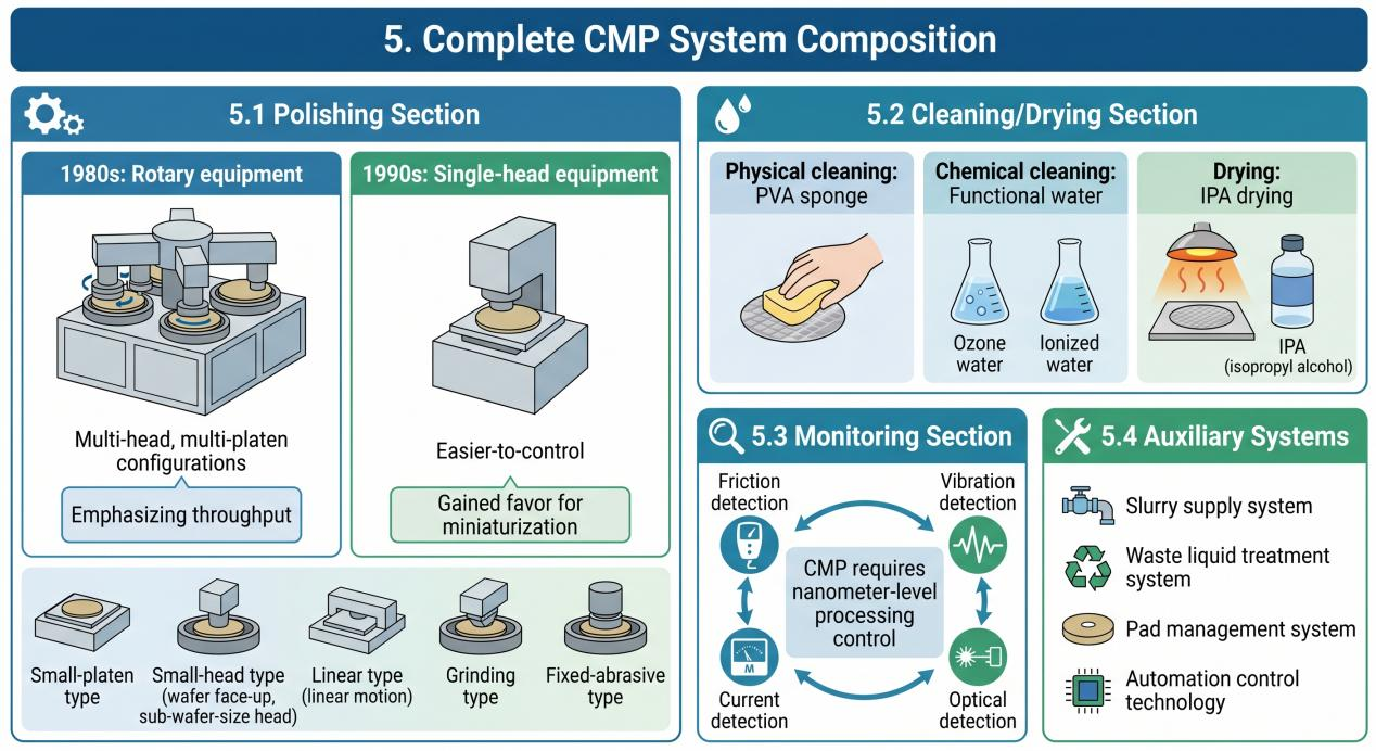
5. Complete CMP System Composition
5.1 Polishing Section
1980s: Rotary equipment dominated, emphasizing throughput with multi-head, multi-platen configurations
1990s: As miniaturization requirements intensified, easier-to-control single-head equipment gained favor
Innovative designs: Small-platen type, small-head type (wafer face-up with sub-wafer-size head), linear type (linear motion), grinding type, and fixed-abrasive type
5.2 Cleaning/Drying Section
Physical cleaning: PVA sponge
Chemical cleaning: Functional water (ozone water, ionized water)
Drying: IPA (isopropyl alcohol) drying
5.3 Monitoring Section
CMP requires nanometer-level processing control. Monitoring methods include:
Friction detection
Vibration detection
Current detection
Optical detection
5.4 Auxiliary Systems
Slurry supply system
Waste liquid treatment system
Pad management systemAutomation control technology
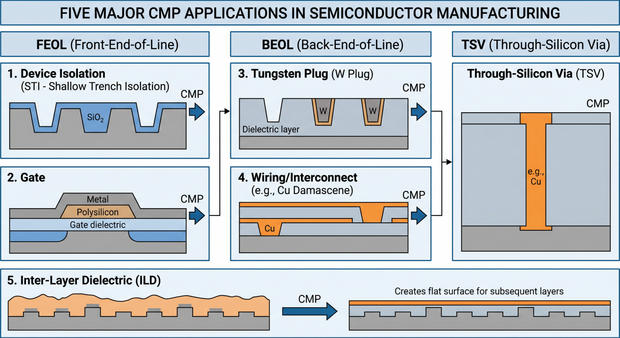
6. Five Major CMP Applications
CMP applications cover Front-End-of-Line (FEOL), Back-End-of-Line (BEOL), and Through-Silicon Via (TSV) processes. The five major applications include:
Device Isolation (STI – Shallow Trench Isolation) — the earliest application, replacing LOCOS technology to resolve lateral scaling issues
Gate
Tungsten Plug (W Plug)
Wiring/InterconnectInter-Layer Dielectric (ILD)
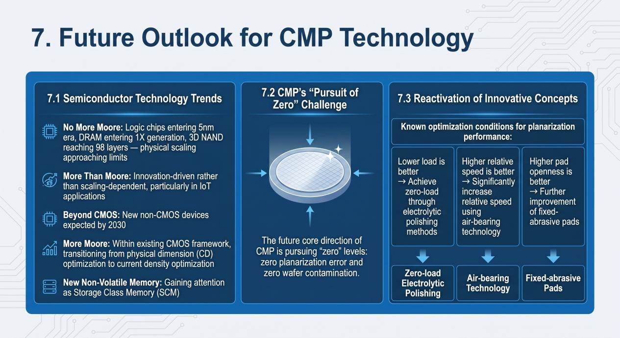
7. Future Outlook for CMP Technology
7.1 Semiconductor Technology Trends
No More Moore: Logic chips entering 5nm era, DRAM entering 1X generation, 3D NAND reaching 98 layers — physical scaling approaching limits
More Than Moore: Innovation-driven rather than scaling-dependent, particularly in IoT applications
Beyond CMOS: New non-CMOS devices expected by 2030
More Moore: Within existing CMOS framework, transitioning from physical dimension (CD) optimization to current density optimization
New Non-Volatile Memory: Gaining attention as Storage Class Memory (SCM)
7.2 CMP’s “Pursuit of Zero” Challenge
The future core direction of CMP is pursuing “zero” levels: zero planarization error and zero wafer contamination.
7.3 Reactivation of Innovative Concepts
Known optimization conditions for planarization performance:
Lower load is better → Achieve zero-load through electrolytic polishing methods
Higher relative speed is better → Significantly increase relative speed using air-bearing technologyHigher pad openness is better → Further improvement of fixed-abrasive pads
8. Core Insights
The successful development of CMP technology reveals that innovation depends not only on technological advancement but also on market explosive power. The “Dry-in/Dry-out” concept was not a breakthrough in polishing technology itself but rather a revolution in usability, which triggered the explosion of the entire market. CMP has become one of the most important forces transforming semiconductor device manufacturing in the 21st century.